Definition: MOSFET (Metal-Oxide-Semiconductor Field-Effect Transistor) is a voltage-controlled device used for switching and amplification.
Key Advantage: High input impedance, low power consumption, and fast switching speeds compared to BJTs.
Types: Divided into N-Channel/P-Channel and Enhancement/Depletion modes.
Selection: Use MOSFETs for high-frequency, low-voltage (<600V) applications; use IGBTs for high-voltage/current.
The MOSFET is a fundamental semiconductor device that utilizes the field effect principle to control current. Compared to traditional bipolar transistors (BJTs), MOSFETs offer high input impedance, low noise, wide dynamic range, and ease of integration.
They are ubiquitous in modern electronics, powering everything from computer power supplies (Switching Power Supplies) to high-frequency inverters and communication devices.
Types and Structure of MOSFETs
MOSFETs act as a specific type of FET (Field Effect Transistor). They are categorized into four distinct types based on their channel and mode of operation:
N-Channel Enhancement Mode (Most common)
N-Channel Depletion Mode
P-Channel Enhancement Mode
P-Channel Depletion Mode

Figure 1: The 4 Classifications of MOSFETs
Every MOSFET has three main electrodes:
G (Gate): The control pin.
S (Source): The current source.
D (Drain): The current output.

Figure 2: Internal Structure of a MOSFET
Ⅰ. MOSFET Working Principle
1. N-Channel Enhancement Mode
This is the most widely used structure. It involves two highly doped N-type regions diffused onto a P-type substrate.
When VGS = 0: No current flows because the P-substrate creates back-to-back PN junctions between the Drain and Source.
When VGS > 0: A positive voltage at the Gate attracts electrons to the surface of the P-substrate. When this voltage exceeds the Threshold Voltage (Vth), an "inversion layer" forms, creating a conductive N-channel connecting the Drain and Source.

Figure 3: N-Channel Enhancement Mode Structure (OFF vs ON)
Pinch-off Effect: As the Drain-to-Source voltage (VDS) increases, the channel becomes tapered. If VDS becomes too high, the channel "pinches off" near the drain, limiting the current. This is the saturation region.

Figure 4: Formation of the Conductive Channel

Figure 5: The Pinch-off Phenomenon
2. P-Channel Enhancement Mode
The operation is the inverse of the N-Channel. It is built on an N-type substrate. To turn it on, the Gate voltage must be lower than the Source voltage (negative VGS) to attract holes and form a channel.

Figure 6: P-Channel Enhancement Mode Structure

Figure 7: P-Channel Channel Formation

Figure 8: P-Channel Pinch-off Region
3. Depletion Mode (N & P)
Unlike enhancement mode, Depletion Mode MOSFETs are "Normally ON" devices. A channel is physically implanted during manufacturing. They conduct current when VGS = 0. To turn an N-Channel depletion MOS off, you must apply a negative gate voltage.
Note: Enhancement mode MOSFETs are preferred in 99% of modern power applications (like switching power supplies) because "Normally OFF" is safer for circuit design.

Figure 9: Depletion Mode Structure and Transfer Characteristics
Ⅱ. Important Characteristics of MOSFETs
1. Switching (Conduction) Characteristics
NMOS: Turns ON when VGS > Vth. Used for Low-Side Switching (Source connected to GND).
PMOS: Turns ON when VGS < Vth. Used for High-Side Switching (Source connected to VCC).
2. Loss Characteristics
MOSFET efficiency is defined by two types of losses:
Conduction Loss: Caused by the internal resistance ($R_{DS(on)}$) when the device is on. $P = I^2 \times R_{DS(on)}$.
Switching Loss: Occurs during the transition between ON and OFF states. Higher frequency = Higher switching loss.
3. Parasitic Capacitance & Driving
MOSFETs have parasitic capacitances (Cgs, Cgd, Cds). Driving a MOSFET essentially means charging and discharging these capacitors. The Miller Effect (Cgd) significantly impacts switching speed.

Figure 10: Comparison of MOSFET Types
4. Parasitic (Body) Diode
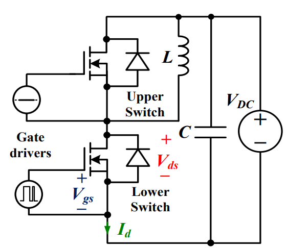
All discrete power MOSFETs have an intrinsic body diode between the Drain and Source. This is crucial for inductive load driving (like motors) as it provides a freewheeling path for current protection.

Figure 11: Position of the Parasitic Body Diode
Ⅲ. MOSFET vs. BJT vs. IGBT
Understanding when to use which device is critical for circuit design.
1. MOSFET vs. BJT (Triode)
| Feature | BJT (Bipolar Junction Transistor) | MOSFET |
|---|---|---|
| Control Type | Current Controlled (Requires Base Current) | Voltage Controlled (Requires Gate Voltage) |
| Switching Speed | Slower (Storage time issues) | Very Fast (No carrier storage time) |
| Input Impedance | Low | Very High |
| Carrier Type | Bipolar (Electrons & Holes) | Unipolar (Majority carriers only) |
| Thermal Stability | Risk of Thermal Runaway (Negative Coeff) | Good (Positive Temp Coeff - Self regulating) |
2. MOSFET vs. IGBT
The IGBT (Insulated Gate Bipolar Transistor) is a hybrid device combining the input characteristics of a MOSFET (Voltage drive) with the output characteristics of a BJT (High current capability).
Low Voltage (< 600V) & High Frequency: MOSFETs are superior due to lower switching losses and linear conduction voltage drop.
High Voltage (> 600V) & High Current: IGBTs are superior. They handle high voltages better but switch slower than MOSFETs.
Ⅳ. Main Parameters of MOSFETs
When reading a datasheet, focus on these critical specifications:
1. Absolute Maximum Ratings
$V_{DSS}$ (Drain-Source Breakdown Voltage): The maximum voltage the device can withstand before breakdown.
$V_{GS}$ (Gate-Source Voltage): Maximum voltage for the Gate oxide layer (usually ±20V). Exceeding this destroys the device.
$I_D$ (Continuous Drain Current): Maximum current the chip can handle at a specific case temperature.
EAS (Single Pulse Avalanche Energy): The device's ability to absorb transient energy (voltage spikes).

Figure 16: Drain Current Limits

Figure 17: Avalanche Test Circuit
2. Static Characteristics
$R_{DS(on)}$ (On-Resistance): The most critical efficiency parameter. Lower resistance means less heat and less power loss.
$V_{GS(th)}$ (Threshold Voltage): The voltage required to start conducting. Logic level MOS (3.3V/5V) has lower thresholds.
3. Dynamic Characteristics
$Q_g$ (Total Gate Charge): The amount of charge required to turn the MOSFET on. Lower $Q_g$ enables faster switching speeds.
$C_{iss}$ (Input Capacitance): Affects how much current the driver needs to supply.
SOA (Safe Operating Area): A graph defining the safe combinations of Voltage and Current to avoid device destruction.


 Product
 Brand
Brand Articles
 Tools
Tools


